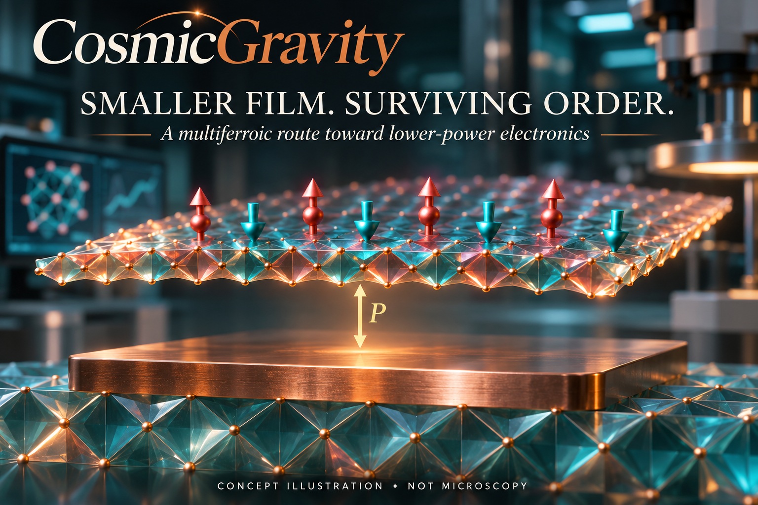
Ultrathin Bismuth Ferrite Breaks a Barrier for Lower-Power Electronics
Ultrathin bismuth ferrite addresses a frustrating problem in electronics: a material can have attractive properties in a laboratory sample and lose them when engineers make it small enough for a device. A Brown University-led team now reports a way to preserve both electrical and magnetic order in exceptionally thin films.
The work, published in Nature Materials on 28 October 2026, concerns the material itself. It offers a possible route towards lower-power memory and logic components. It does not yet show a finished AI processor or a measured reduction in a data centre’s electricity bill.
Why ultrathin bismuth ferrite matters
Bismuth ferrite belongs to a class called magnetoelectric multiferroics. In practical terms, the attraction is a connection between electrical and magnetic behaviour in the same material. That creates possibilities for controlling a state electrically and detecting it through a magnetic response.
Brown’s account of the research explains the memory idea through electrical polarization: the arrangement of positive and negative charge within a crystal. A voltage can reverse that arrangement. Distinguishable states can, in principle, represent stored information.
The appeal is therefore understandable. If a useful device can write and read information while moving less charge or wasting less energy, that could help reduce the cost of computation. But the word “if” carries engineering work. A material with switchable properties and an efficient electronic component are different milestones.
The dead-layer problem
Making a film thinner changes the importance of its surfaces and interfaces. The published study’s abstract identifies several ways in which useful order can fail, including electrical depolarization and changes that undermine magnetism. A film may retain its chemical name while losing the behaviour engineers wanted from it.
That is what makes a “dead layer” more than a manufacturing inconvenience. Adding less material is not a successful miniaturisation strategy if the resulting structure no longer performs its essential function.
The terminology is also easy to overread. “Dead” describes a loss of the properties at issue, not literal inactivity in every possible sense. Similarly, removing this limitation in a particular engineered system does not establish that all thin-film materials have overcome their own scaling problems.
How the team engineered ultrathin bismuth ferrite
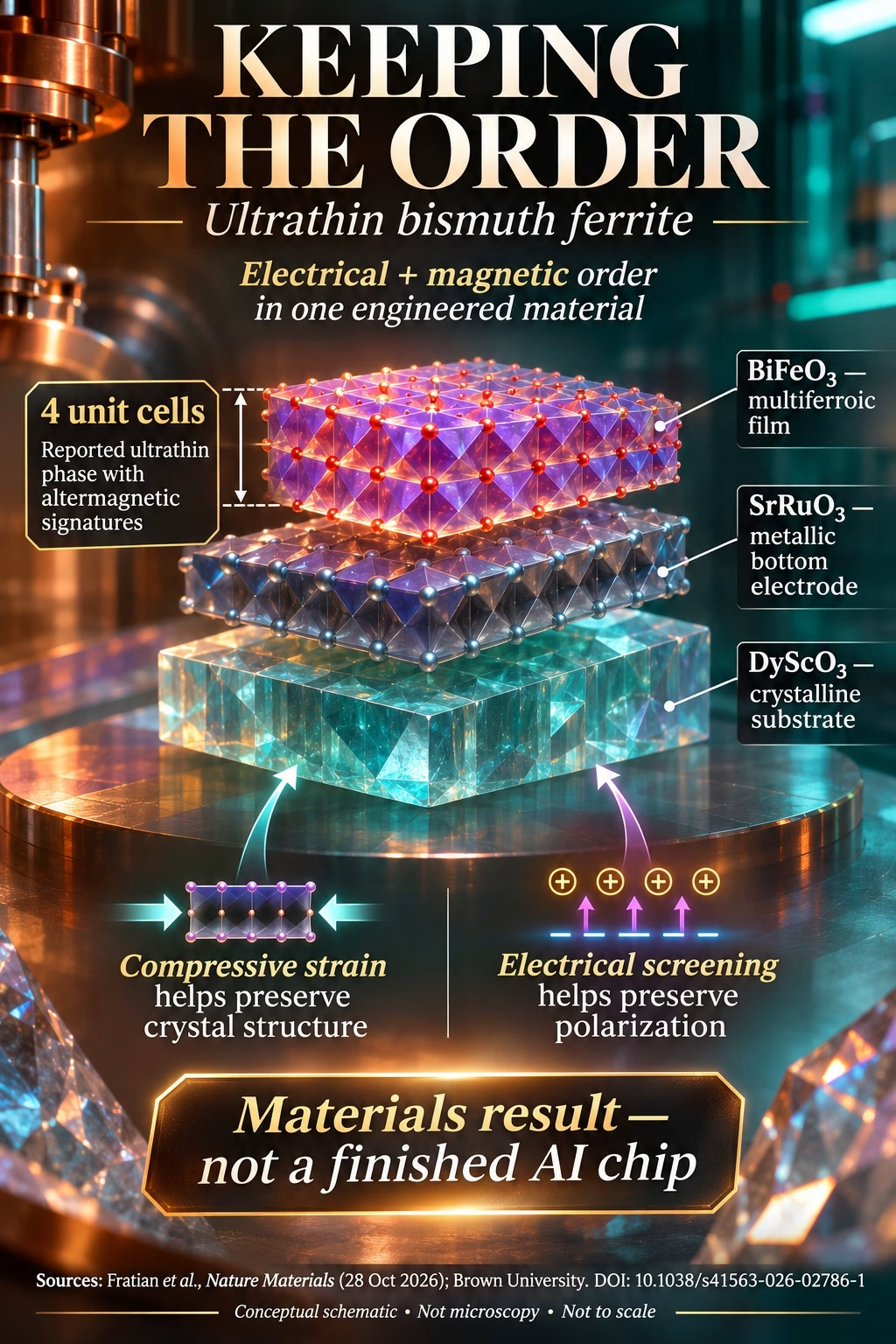
The approach combines strain with control of the electrical environment. The film grows on a carefully chosen crystalline foundation, with a metallic bottom electrode. These interfaces help maintain the conditions needed for the film’s electrical and magnetic behaviour.
The authors’ public manuscript describes the role of epitaxial strain and short-circuit electrical boundary conditions. Its methods and figure captions identify bismuth ferrite, a strontium ruthenate bottom electrode and a dysprosium scandate substrate. Those names matter because the result comes from an engineered structure, rather than from simply shaving a bulk crystal thinner.
Think of the surrounding layers as part of the experiment’s design. The foundation constrains how the crystal fits; the electrical surroundings influence whether polarization can survive. Neither role is captured by a headline that says only that a new magnet is smaller.
Four unit cells and altermagnetic signatures
The published abstract reports a phase at four unit cells with signatures of altermagnetic order. A unit cell is a repeating building block of a crystal. Counting these blocks describes the film’s thickness; it does not describe the size of an entire transistor, chip or memory array.
The distinction matters because electronics headlines often put several kinds of “small” next to one another. A thin active material still needs contacts, neighbouring structures and a means of writing and reading information. The scale of one layer is not a specification for a finished product.
Altermagnetism adds another interesting possibility. A recent Nature Physics review describes this form of magnetic order and its relevance to spintronics, a field that uses electron spin in electronic functions. The attraction includes spin-dependent behaviour without the conventional net magnetization associated with an everyday permanent magnet.
For this study, the useful formulation is the authors’ own: altermagnetic signatures supported by several investigative methods. That includes magnetic measurements, imaging and calculations. It is stronger than judging the material from one attractive microscopic image, while still leaving device performance as a separate question.
What would make this useful in a chip?
The next questions are concrete. Can engineers switch and read the relevant states reliably? How much energy does each operation require? How well does the structure tolerate repeated use, temperature changes and the processes used to build neighbouring components?
These are questions for further work, not failures demonstrated by this paper. They explain why an important materials result can deserve attention before a commercial device exists. Preserving useful order removes one obstruction; it does not automatically remove every later one.
Our report on an optical AI chip explores a different route through computing hardware. Our article on a self-controlling silicon quantum processor concerns another technology again. Their headline figures cannot serve as benchmarks for this thin film: the systems perform different jobs and have reached different stages of development.
A route forward for ultrathin bismuth ferrite
The public manuscript first appeared in January and received an October revision; the journal article and manuscript belong to the same investigation. The publication date marks the peer-reviewed record, not an independent replication by a second team.
What the work contributes is a way to keep desirable order alive as a multiferroic film becomes extremely thin. That makes the next engineering questions worth asking. The prospect of lower-power electronics is the motivation; the surviving electrical and magnetic order is the result researchers can examine now.
Research checked 2 November 2026. Primary references distinguish the reported film properties from future computing applications. Conceptual graphics are original to CosmicGravity and do not reproduce experimental images.

latest video



news via inbox
Subscribe to our Cosmic newsletter to get notified when we have new articles.